3C Electronics

Stamping technology is widely used in the 3C electronics industry. Here are several key applications in the 3C electronics industry:
Assembly of small components: such as inserting connectors into PCBs (Printed Circuit Boards), assembling mobile phone parts, and mounting microprocessors onto motherboards.
Metal cases: Stamping presses can perform bending, stamping and forming operations with high precision for applications such as smartphone, tablet and laptop casings and keyboards.
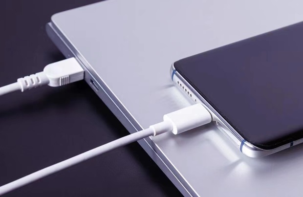
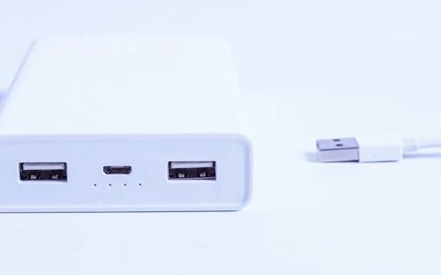
Connector Manufacturing: Connectors are an essential component in electronic devices for signal and power transmission. Stamping presses also play an important role in the manufacturing process of electronic connectors, such as USB plugs and HDMI interfaces.
Screen Bonding and Lamination: The application of uniform pressure across screens during bonding or lamination processes is critical for avoiding bubbles and ensuring adhesion.

Battery Assembly and Testing: In the production of batteries for electronic devices, stamping presses can be used for tasks such as welding battery tabs, assembling battery packs, and performing compression tests on batteries to ensure their safety and reliability.
Microelectromechanical Systems (MEMS): The precise force application provided by stamping presses is used in the fabrication and assembly of MEMS, including the various sensors and actuators within electronic devices.
Testing and Quality Control: Stamping presses are used in testing components for mechanical strength, such as button durability tests, bend tests for flexibility, and impact resistance tests.
Circuit Board Processing: Stamping presses can carry out the lamination of multilayer boards, drilling of core boards, and other processes required in the manufacturing of 3C electronic products' circuit boards.


